Wafer AOI Designed for Wafer and Sawn Wafer Configuration
.png)
Product image
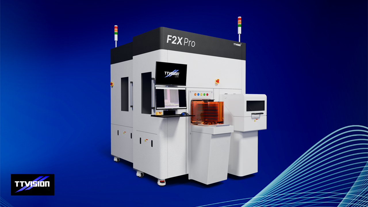
Wafer AOI Designed for Wafer and Sawn Wafer Configuration
Description
Built for advanced semiconductor front-end and back-end packaging, the F2X Pro delivers rapid yield assurance and micro-defect detection across complex die surfaces, probe marks, saw lines, and bumps.
Features
- Wafer & Sawn Wafer Compatibility:
Built to inspect both whole wafers and dicing film-mounted sawn wafers with minimum to zero mechanical tool conversion between product changes, maximizing equipment uptime. - Comprehensive Multi-Process Defect Coverage:
Inspects for surface contamination/scratches, probe mark integrity, sawing chipping/crack defects, and bump micro-anomalies (height, bridge, missing bumps) on a single platform. - Hybrid Dual-Gate Detection (Rule & AI-Based):
Combines high-speed, deterministic rule-based inspection algorithms with advanced AI deep-learning models to reliably identify subtle, non-standard defects while drastically reducing false overkills. - High-Stability Optomechanical Foundation:
Built on a heavy vibration-isolated granite motion stage that eliminates ambient shop-floor micro-vibrations, enabling sub-micron accuracy during high-speed scanning. - Multi-Magnification & Multi-Illumination System:
Integrates dynamic multi-channel illumination (brightfield, darkfield, oblique) and multi-magnification optical lenses to render fine defect contrast regardless of substrate reflectivity or topography. - Auto Defect Classification (ADC) & Review Software:
Includes built-in AI algorithms to instantly classify defect types and an intuitive review software interface for rapid offline verification and statistical process control (SPC) tracking. - Scalable Performance Upgrades:
Features a modular architecture that allows field upgrades for higher optics resolution, speed boosts, or expanded software capabilities as production requirements grow.