Wafer AOI Machine
.png)
Product image
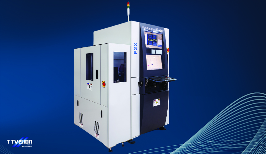
Wafer AOI Machine
Description
The Wafer AOI Machine is an essential tool for maintaining the highest levels of quality control in semiconductor manufacturing, ensuring the reliability and performance of the final products.
Features
- 5S Surface Inspection:
The Wafer AOI Machine is equipped with advanced 5S surface inspection technology. This comprehensive system thoroughly examines the wafer's surface, detecting and analyzing defects related to sawing, metallization, and other surface irregularities. - Auto Focus Module:
Incorporating an auto-focus module, the machine ensures precise and consistent focusing during the inspection process. This feature contributes to enhanced accuracy and detailed defect identification across the wafer's surface. - Modular Design:
The machine features a modular design, offering versatility and adaptability in its configuration. This design enables easier maintenance, upgrades, and customization to accommodate varying inspection requirements and future technological advancements. - 64-Bit OS & i9 Processor:
Powered by a 64-bit operating system and an i9 processor, the Wafer AOI Machine operates on robust and high-performance hardware, ensuring swift processing of inspection data and efficient handling of complex algorithms. - High Throughput and Camera Resolution:
With a remarkable throughput capability of up to 16 Wafers Per Hour (WPH), this machine offers efficient and rapid inspection cycles. The camera resolution, reaching up to 25 megapixels, guarantees detailed and high-definition imaging for precise defect identification. - Exceptional Accuracy:
Achieve remarkable accuracy in defect detection, with a precision of up to 0.55 micrometers per pixel. This high level of accuracy ensures reliable identification and classification of even the smallest defects on the wafer's surface. - Multiple Reject Handling (EMAP, Inking):
The machine provides multiple reject handling mechanisms such as EMAP and inking, facilitating efficient sorting and handling of rejected wafers based on identified defects. This feature streamlines the rejection process for further analysis or removal. - Robot Arm Material Handling:
Integrated with a robot arm for material handling, the machine ensures seamless and automated transfer of wafers throughout the inspection process. This automation optimizes workflow efficiency and reduces manual intervention, enhancing overall productivity.
Application
-
Post Saw Inspection:
The Wafer AOI Machine is specifically designed for post-saw inspection, ensuring that wafers undergo meticulous scrutiny after the sawing process to detect any surface defects. -
Singulated Package Inspection:
With a focus on singulated package inspection, the machine ensures the quality and integrity of individual semiconductor packages, contributing to the overall reliability of the end product.