Substrate Package AOI Machine
.png)
Product image
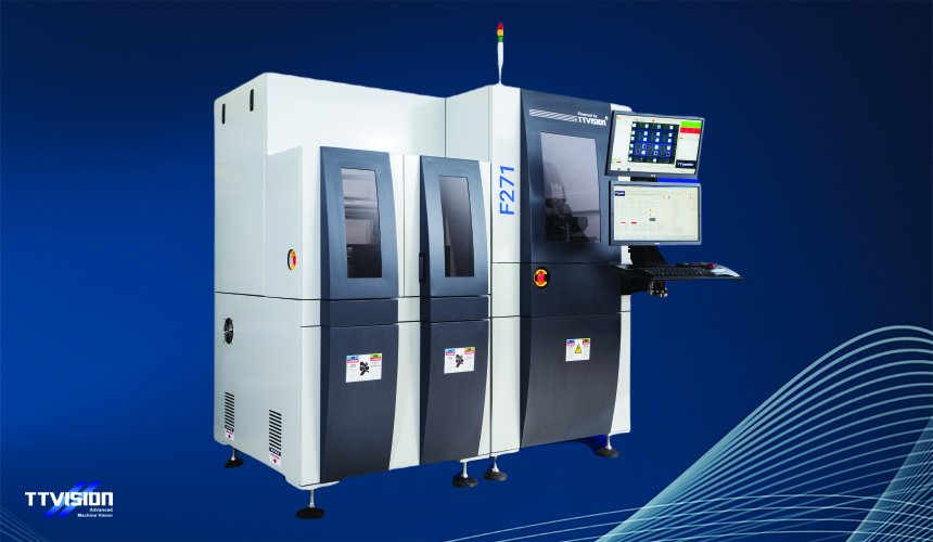
Substrate Package AOI Machine
Description
The Substrate Package AOI Machine plays a crucial role in maintaining the highest standards of quality control in semiconductor manufacturing, making it an indispensable asset for your production line.
Features
- Line Scan Technology:
The Substrate Package AOI Machine incorporates state-of-the-art line scan technology, ensuring high-precision inspection across the entire surface. This technology enables a continuous scan, capturing detailed images for thorough and accurate defect detection. - 2D Auto Inspection:
Benefit from automated two-dimensional inspection capabilities that enhance the efficiency and reliability of the inspection process. The machine's advanced algorithms analyze images in real-time, identifying and categorizing defects with precision. - Very Fast Large Panel Inspection:
Experience unparalleled speed in large panel inspection. The machine's advanced capabilities allow for swift and thorough inspection of large substrate panels, optimizing production efficiency without compromising accuracy. - Throughput up to 500 Strips per Hour:
Achieve impressive throughput with the Substrate Package AOI Machine, processing up to 500 strips per hour. This high throughput ensures that your production line maintains efficiency without sacrificing the quality of inspection. - Camera Resolution of 16000 Pixels at 47.5KHz Max Line Rate:
Benefit from superior imaging capabilities with a high-resolution camera, boasting 16,000 pixels at a maximum line rate of 47.5KHz. This ensures the capture of exceptionally detailed images, crucial for detecting even the smallest defects in substrates.
Application
-
Etching Defects:
Detect and analyze etching defects with precision, ensuring the integrity of the substrate surface and preventing potential issues in downstream processes. -
Mechanical Defects:
Thoroughly inspect for mechanical defects, such as cracks or deformities, guaranteeing the structural soundness of the lead frame substrate. -
Plating Defects:
Identify and address plating defects, ensuring the uniformity and quality of the plating process. This contributes to the overall reliability and performance of the final semiconductor components.